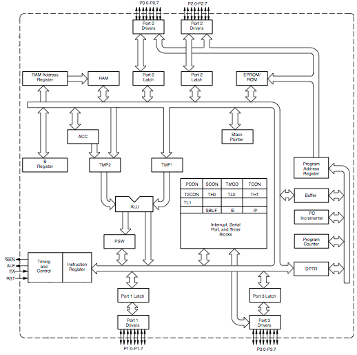
Description
One of the best supported and most widely used types of embedded CPUs is Intel‘s MCS 51 series of devices. This is enough reason to create an 8051-compatible CPU core for FPGA usage. Use of this core makes very much sense when porting existing designs to FPGA technology, or as an easy-to-adapt reference application.

Features
- cycle compatible to MCS 51
- supported by a wide range of development tools
- very compact design
- on-chip 128 byte data RAM
- minimum gate count
- optimized for FPGA implementation
- lowest possible design risk
- free behavioral model
- comprehensive reference application
- synthesizable VHDL model
- very low cost
Synthesis
The core was successfully synthesized with Synopsys FPGA Express and Xilinx XST. This is a summary of the required resources:
- total number of 4 input LUTs: 1,934
- number used as LUTs: 1,846
- number used as route-thru: 24
- number used as 32×1 RAMs: 64
- number of slice flip flops: 353
- total equivalent gate count: 23,299
Verification
The CPU core was verified on several levels:
- simulation of every single instruction
- simulation of test programs
- real-life test with reference applications
Resources: